Starfield 登陸 PS5:4 月 7 日發售完整指南,Xbox 獨占時代正式終結
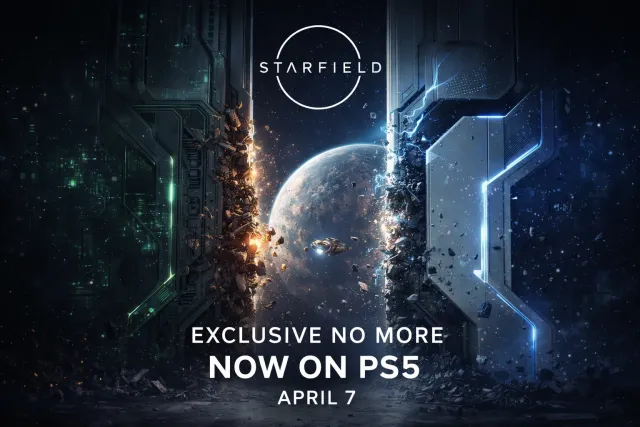
Bethesda 的太空 RPG 大作 Starfield 將於 2026 年 4 月 7 日登陸 PS5,同步帶來首個 DLC 擴展包 Shattered Space、新 DLC Terran Armada 以及大型免費更新 Free Lanes。本文整理 PS5 版本規格、新增內容與從零開始的入門指南。
Bethesda 的太空 RPG 大作 Starfield 將於 2026 年 4 月 7 日登陸 PS5,同步帶來首個 DLC 擴展包 Shattered Space、新 DLC Terran Armada 以及大型免費更新 Free Lanes。本文整理 PS5 版本規格、新增內容與從零開始的入門指南。
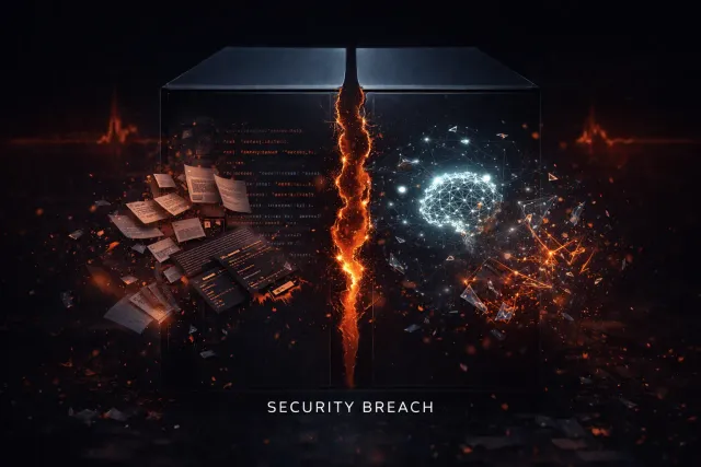
2026 年 3 月 26 日至 31 日,Anthropic 在短短七天內發生兩起重大資安事件:內部未發布的 Mythos 模型細節遭到洩露,緊接著 Claude Code v2.1.88 的 51 萬行源碼透過 npm 打包錯誤公開流傳。本文整理完整事件經過、外洩內容、潛在風險與 Anthropic 的官方回應。
Avowed 正式發售三個月後,本文從世界觀、戰鬥系統、角色扮演深度和技術面全面評析。Obsidian Entertainment 能否在 Bethesda 和 CD Projekt Red 之後,打造出屬於自己的 RPG 聖殿?

2026 年 AI 程式開發工具三強鼎立:Claude Code、Cursor 和 GitHub Copilot 各有優勢。本文從實際開發工作流出發,用具體數據和場景測試,告訴你哪款工具最適合你的需求。
Google DeepMind 在 2026 年 3 月 3 日正式發布 Gemini 2.0 Ultra,主打原生多模態推理與百萬 token 上下文。本文用最新基準測試與實戰場景,帶你全面了解 Gemini 2.0 Ultra 的真實實力。
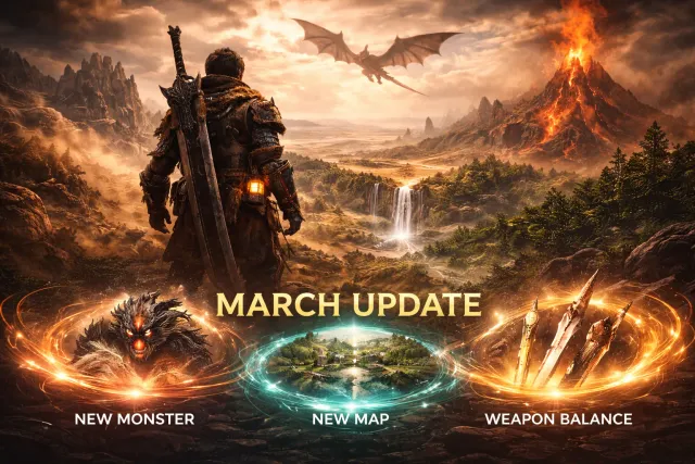
Monster Hunter Wilds 2026 年 3 月大型更新正式上線,帶來全新古龍「迷域龍」、新地圖「沉息谷」及大規模武器平衡調整。本文整理所有更新內容與最強武器配置推薦。
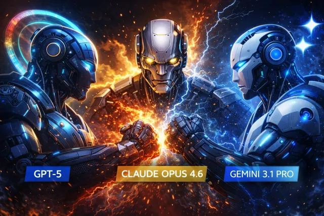
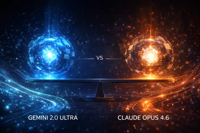
2026 年 2 月是 AI 競賽最激烈的一個月。GPT-5.3、Claude Opus 4.6、Gemini 3.1 Pro 同步較勁,DeepSeek V4 從側翼殺入。本文用最新基準測試數據,告訴你各模型的真實強項與最佳使用場景。
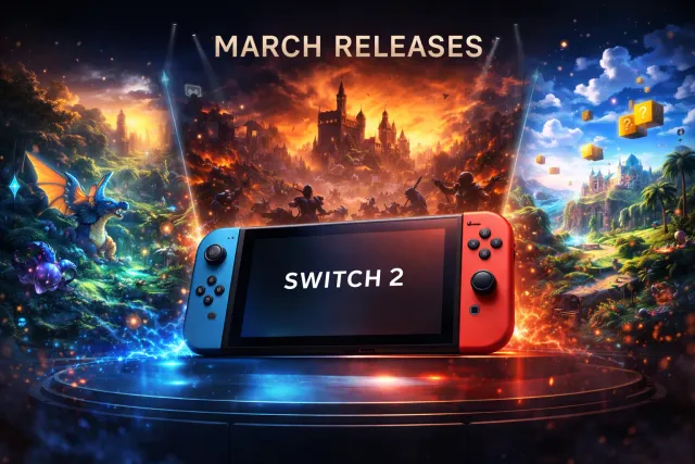
Nintendo Switch 2 三月陣容正式確定,Pokemon Pokopia、惡靈古堡:蝴蝶之殤 Remake、Monster Hunter Stories 3 等 8 款大作齊發。本文整理完整發售時間、遊戲亮點,以及 Switch 2 目前的熱銷現況。
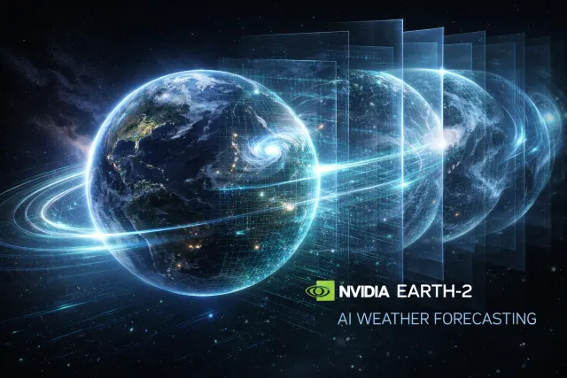
NVIDIA 發布 Earth-2,全球首個完全開源的 AI 天氣預報平台。三大模型涵蓋全球中期預報、局部暴風預測和大氣數據同化,將傳統超級電腦需要數小時的運算壓縮到幾秒鐘完成。

《人中之龍 極 3 & Dark Ties》於 2 月 12 日正式發售。本作包含經典重製與全新前傳兩款遊戲,新增龍宮流戰鬥風格、飆車女王模式和地下格鬥場。本文整理評測分析、系統詳解與新手建議。
AI 模型像黑箱一樣運作,沒人知道它為什麼這樣回答。機械可解釋性正在改變這一點。MIT Technology Review 將其列為 2026 十大突破技術,Anthropic 已能追蹤 Claude 從輸入到輸出的完整思考路徑。
Sony 確認 PlayStation State of Play 將於 2 月 12 日登場,長達 60 分鐘以上。Marvel's Wolverine 的完整展示、Marathon 最新進度、Naughty Dog 新作 Intergalactic 都可能亮相。本文整理所有已知資訊與預測。